Posts

Showing posts from July, 2021

Frequency Divider & Counters

Image
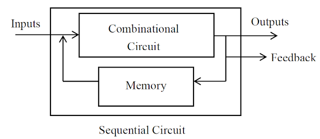
 Frequency Divider A frequency divider can be constructed from J-K flip-flops by taking the output of one cell to the clock input of the next. The J and K inputs of each flip-flop are set to 1 to produce a toggle at each cycle of the clock input. For each two toggles of the first cell, a toggle is produced in the second cell, so its output is at half the frequency of the first. The output of the fourth cell is 1/16 the clock frequency. The same device is useful as a binary counter. Simulation of Frequency Divider Counters A counting circuit composed of memory elements, such as flip-flops and electronic gates, is the simplest form of sequential circuit available. All sequential circuits are of two types,  synchronous (clock driven)  asynchronous (event driven) In synchronous circuits, changes in the circuit state are synchronised to the normally periodic clock pulses, whereas in event driven circuits state changes are governed by events such as, for example, the occurrence of a system f

Flip - Flops

Image
The basic difference between a latch and a flip-flop is a gating or clocking mechanism. In Simple words, Flip Flop is edge-triggered and a latch is level triggered. S-R Flip Flop This simple flip-flop circuit has a set input (S) and a reset input (R). In this system, when you Set “S” as active the output “Q” would be high and “Q‘” will be low. Once the outputs are established, the wiring of the circuit is maintained until “S” or “R” go high, or power is turned off. As shown above, it is the simplest and easiest to understand. The two outputs, as shown above, are the inverse of each other. Truth Table for S-R Flip flop Simulation of S-R Flip flop J-K Flip flop The JK Flip-flop is similar to the SR Flip-flop but there is no change in state when the J and K inputs are both LOW. Truth Table for J-K Flip Flop Simulation for J-K Flip Flop

Sequential Logic circuit

Image
Sequential Logic circuits are also combinational logic circuits with memory. The output of a Sequential Logic circuit is depending on present input and also on the present state of the memory. Information which is stored in the memory is identified as present state. The present state is defined the present output and next state also. S - R Latch For getting the output from SR Latch we have consider not only S and Inputs but also we have consider Qn current state. S - R Latch Truth Table x = Don't no the value Simulation of S - R Latch

2-bit Multiplier

Image
 A Binary Multiplier is a digital circuit used in digital electronics to multiply two binary numbers and provide the result as output. The method used to multiply two binary numbers is similar to the method taught to school children for multiplying decimal numbers which is based on calculating partial product, shifting them and adding them together. Similar approach is used to multiply two binary numbers. Long multiplicand is multiplied by 0 or 1 which is much easier than decimal multiplication as product by 0 or 1 is 0 or same number respectively. Truth Table for 2-bit Multiplier Simulation for 2 - bit Multiplier

Introduction to CEDAR Logic Simulator

Image
 Cedar Logic simulator also like Logisim simulator but in Logisim there is no time diagram. So next chapters will cover using Cedar logic simualtor. How to download & Install Cedar Logic Simulator You can simply download it from here - Download Now Installation is easy, It didn't require any additional software to download. Overview of CEDAR Logic Simulator

Multiplexers & De-multiplexers

Image
Multiplexer Multiplexer is a combinational logic circuit designed to switch one of several input lines to a single common output line. 2 to 1 Multiplexer The input A of this simple 2-1 line multiplexer circuit constructed from standard NAND gates acts to control which input ( I0 or I1 ) gets passed to the output at Q. Simulation of 2 to 1 Multiplexer 4 to 1 Multiplexer 4 to 1 Multiplexer Using NAND gates Simulation of 4 to 1 Multiplexer De-multiplexers The demultiplexer is a combinational logic circuit designed to switch one common input line to one of several seperate output line. 1-to-4 Channel De-multiplexer & truth table Simulation of 1 to 4 De-multiplexer

Encoders & Decoders

Image
Encoders  Encoder is a combinational circuit which have multiple inputs and multiple outputs circuit. If we have n number of inputs we can get n = 2m. So number of outputs are equal to9 m.            Example: number of inputs are 4; 4 = 22. So number of outputs are 2. There are 4 types of encoders. Priority Encoder Decimal to BCD Encoder Octal to Binary Encoder Hexadecimal to Binary Encoder Priority Encoder Priority Encoders take all of their data inputs one at a time and converts them into an equivalent binary code at its output. 4 to 2 Bit Binary encoder & Truth table Simulation of 4 tot 2 encoder vid here Decoders Decoder is a combinational circuit which have multiple inputs and multiple outputs circuit. It decodes n inputs into 2n outputs. Example: number of inputs are 2, number of outputs are 22 = 4. E is used to enable or disable the circuit. If E = 0, the circuit is disabled and if E = 1, the circuit is abled. 2 to 4 Binary Decoder & Truth table 2 to 4 Binary Decoder Sim

Binary Subtractor

Image
 The Binary Subtractor is another type of combinational arithmetic circuit that produces an output which is the subtraction of two binary numbers Half Subtractor A half subtractor is a logical circuit that performs a subtraction operation on two binary digits. The half subtractor produces a sum and a borrow bit for the next stage. Simulation of Half Subtractor Full Subtractor As the full subtractor circuit above represents two half subtractors cascaded together, the truth table for the full subtractor will have eight different input combinations as there are three input variables, the data bits and the Borrow-in, BIN input. Also includes the difference output, D and the Borrow-out, BOUT bit. Simulation of Full Subtractor

Adders

Image
Binary Adders are arithmetic circuits in the form of half-adders and full-adders used to add together two binary digits Half adder Half adder is a combinational circuit which is designed for adding two single bit numbers. Single bit number means 1 and 0. Half adder contain 2 inputs and 2 outputs. Truth table for half adder Simulation of Half adder Full adder Full adder is used to add numbers which have more single bit numbers. It is consisting of collection of half adders. Full adder has 3 inputs, to half adder inputs by adding another input called carry in. Truth table and circuit Simulation of full adder

Combinational Logic circuit

Image
Combinational Logic Circuits are memoryless digital logic circuits whose output at any instant in time depends only on the combination of its inputs Combinational Logic Combinational Logic Circuits are made up from basic logic NAND, NOR or NOT gates that are “combined” or connected together to produce more complicated switching circuits. These logic gates are the building blocks of combinational logic circuits. An example of a combinational circuit is a decoder, which converts the binary code data present at its input into a number of different output lines, one at a time producing an equivalent decimal code at its output. Combinational logic circuits can be very simple or very complicated and any combinational circuit can be implemented with only NAND and NOR gates as these are classed as “universal” gates. The three main ways of specifying the function of a combinational logic circuit are: 1. Boolean Algebra – This forms the algebraic expression showing the operation of the logic c

Logic Gate Simulator Tools and Logisim

Image
 There are many simulator tools available on the internet to do logic gate simulations. Some of them can use online also. Below mention some free simulation tools for logic gate simulation. And also you can download or use them by clicking it. Logisim Ceder Logic Simulator Logicly Deeds Logisim Logic gate Simulator Logisim is a lightweight simulator. This is an educational tool software to design logic gate base implementations. How to Download and install Logisim  You can simply download it from here : Download logisim   Also you want to download Java if you haven't installed it before. Overview Logisim Simulator Now let's take a look at logisim window. When you start logisim, main window elements are like this. There is a toolbar with basic 3 gates.  Hand - You can use this for change input 1 to 0 or 0 to 1. Cursor - This is need for build simulation Rename - For name gates Input  Output NOT gate AND gate OR gate How to Draw, Simulate & Analyze a circuits using Logisim